Product Summary
The XC6VLX240T-1FFG1759C is a member of the Virtex-6 family, which provides the newest, most advanced features in the FPGA market. The XC6VLX240T-1FFG1759C is the programmable silicon foundation for Targeted Design Platforms that deliver integrated software and hardware components to enable designers to focus on innovation as soon as their development cycle begins. Using the third-generation ASMBL (Advanced Silicon Modular Block) columnbased architecture, the XC6VLX240T-1FFG1759C contains multiple distinct sub-families. This overview covers the devices in the LXT, SXT, and HXT sub-families. Each sub-family contains a different ratio of features to most efficiently address the needs of a wide variety of advanced logic designs. In addition to the high-performance logic fabric, Virtex-6 FPGAs contain many built-in system-level blocks. These features allow logic designers to build the highest levels of performance and functionality into their FPGA-based systems. Built on a 40 nm state-of-theart copper process technology, the XC6VLX240T-1FFG1759C is a programmable alternative to custom ASIC technology. Virtex-6 FPGAs offer the best solution for addressing the needs of high-performance logic designers, high-performance DSP designers, and high-performance embedded systems designers with unprecedented logic, DSP, connectivity, and soft microprocessor capabilities.
Parametrics
XC6VLX240T-1FFG1759C absolute maximum ratings:(1)VCCINT: Internal supply voltage relative to GND: –0.5 to 1.1 V; For -1L devices: Internal supply voltage relative to GND: –0.5 to 1.0 V; (2)VCCAUX, Auxiliary supply voltage relative to GND: –0.5 to 3.0 V; (3)VCCO, Output drivers supply voltage relative to GND: –0.5 to 3.0 V; (4)VBATT, Key memory battery backup supply: –0.5 to 3.0 V; (5)VFS External voltage supply for eFUSE programming: –0.5 to 3.0 V; (6)VREF, Input reference voltage: –0.5 to 3.0 V; (7)VIN, 2.5V or below I/O input voltage relative to GND (user and dedicated I/Os): –0.5 to VCCO + 0.5 V; (8)VTS, Voltage applied to 3-state 2.5V or below output(4) (user and dedicated I/Os): –0.5 to VCCO + 0.5 V; (9)TSTG, Storage temperature (ambient): –65 to 150℃; (10)TSOL, Maximum soldering temperature: +220℃; (11)Tj, Maximum junction temperature: +125℃.
Features
XC6VLX240T-1FFG1759C features: (1)Three sub-families; (2)Compatibility across sub-families; (3)Advanced, high-performance FPGA Logic; (4)Powerful mixed-mode clock managers (MMCM); (5)36-Kb block RAM/FIFOs; (6)High-performance parallel SelectIO technology; (7)Advanced DSP48E1 slices; (8)Flexible configuration options; (9)System Monitor capability on all devices; (10)Integrated interface blocks for PCI Express designs; (11)GTX transceivers: up to 6.6 Gb/s ; (12)GTH transceivers: 2.488 Gb/s to beyond 11 Gb/s; (13)Integrated 10/100/1000 Mb/s Ethernet MAC block; (14)40 nm copper CMOS process technology; (15)1.0V core voltage (-1, -2, -3 speed grades only); (16)Lower-power 0.9V core voltage option (-1L speed grade only); (17)High signal-integrity flip-chip packaging available in standard or Pb-free package options.
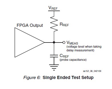
Diagrams

| Image | Part No | Mfg | Description |  |
Pricing (USD) |
Quantity | ||||||
|---|---|---|---|---|---|---|---|---|---|---|---|---|
 |
 XC6VLX240T-1FFG1759C |
 |
 IC FPGA VIRTEX 6 241K 1759FFGBGA |
 Data Sheet |

|
|
||||||
| Image | Part No | Mfg | Description |  |
Pricing (USD) |
Quantity | ||||||
 |
 XC6VCX130T-1FFG1156C |
 |
 IC FPGA VIRTEX 6 128K 1156FFGBGA |
 Data Sheet |

|
|
||||||
 |
 XC6VCX130T-1FFG1156I |
 |
 IC FPGA VIRTEX 6 128K 1156FFGBGA |
 Data Sheet |

|
|
||||||
 |
 XC6VCX130T-1FFG484C |
 |
 IC FPGA VIRTEX 6 128K 484FFGBGA |
 Data Sheet |

|
|
||||||
 |
 XC6VCX130T-1FFG484I |
 |
 IC FPGA VIRTEX 6 128K 484FFGBGA |
 Data Sheet |

|
|
||||||
 |
 XC6VCX130T-1FFG784C |
 |
 IC FPGA VIRTEX 6 128K 784FFGBGA |
 Data Sheet |

|
|
||||||
 |
 XC6VCX130T-1FFG784I |
 |
 IC FPGA VIRTEX 6 128K 784FFGBGA |
 Data Sheet |

|
|
||||||
 (China (Mainland))


